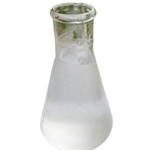
Introduction: The Science of Flow
In the huge and requiring landscape of modern-day building and construction, where structural honesty meets building ambition, there exists a silent catalyst that transforms the impossible right into fact. The Plasticiser is not just an additive; it is the molecular architect of workability, the unnoticeable pressure that determines how concrete flows, collections, and withstands. For years, the industry struggled with the fundamental opposition between stamina and fluidity– until we grasped the chemistry to link this divide. Our brand name was started on the principle that real innovation exists at the microscopic level, where the manipulation of surface area stress can redefine macroscopic efficiency. We do not just offer fluid ingredients; we engineer the rheology of the developed atmosphere. This is the tale of just how we took advantage of the power of advanced plasticisers to transform stiff accumulations right into flowing art, making sure that the foundations of our cities are as resilient as they are splendid. It is a trip from the turmoil of basic materials to the precision of high-performance engineering.
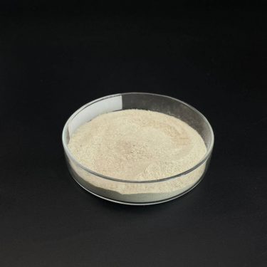
(Plasticiser)
Brand Beginning: Past the Water-Cement Ratio
Our journey started in the early days of industrial construction, a time when builders were shackled by the restrictions of the traditional water-cement proportion. Engineers faced a ruthless trade-off: include water to make the mix workable and sacrifice strength, or maintain it completely dry for stamina and fight unrestrainable tightness. The creators of our brand name, a collective of polymer drug stores and civil designers, contradicted this concession. They believed that the solution lay not in brute force, but in molecular finesse. In a moderate laboratory loaded with beakers and viscometers, they sought to open the possibility of polycarboxylate ether (PCE). They imagined a globe where concrete could flow like water yet remedy like rock.
The Innovation Minute. The turning point came when we successfully manufactured a comb-shaped polymer that could literally press cement fragments apart without the requirement for excess water. This steric hindrance result was advanced. It allowed us to significantly lower water material while at the same time boosting slump and flow. We recognized then that we weren’t just making an item; we were creating a new standard for the market. Our brand arised from these try outs a particular objective: to get rid of the ineffectiveness of standard blending and empower contractors with products that opposed traditional restrictions. We moved from theoretical chemistry to practical application, showing that a few drops of our plasticiser could save lots of concrete and expand the life-span of infrastructure by decades.
Core Process: Design the Interface
The development of a remarkable Plasticiser is a symphony of organic synthesis and colloid chemistry. It calls for an obsessive interest to detail, where the length of a polymer chain or the thickness of a side group can imply the difference in between a groundbreaking solution and a stopped working batch. At the heart of our procedure lies a proprietary production process that guarantees every molecule performs its duty with absolute precision. We do not just mix chemicals; we construct useful structures atom by atom.
Precision Polymerization. Our procedure begins with the free-radical polymerization of specialized monomers. This is carried out in highly regulated activators where temperature and stress are checked down to the decimal point. We utilize innovative implanting strategies to produce the unique “comb” framework of our PCE molecules. The backbone of the molecule anchors itself to the cement particle, while the lengthy side chains prolong outward, producing a safety shield. This certain architecture is what produces the effective dispersing force that specifies our products.
Molecular Weight Control. Among one of the most important facets of our core process is the strict control of molecular weight distribution. A plasticiser with irregular chain sizes will certainly do unpredictably in the area. We employ innovative chromatography to make sure that every batch drops within a slim, enhanced array. This consistency guarantees that whether our plasticiser is used in a high-rise in Dubai or a bridge in Norway, the performance remains similar. It is this integrity that has made us the trusted partner of the world’s leading precast manufacturers.
Customized Functionalization. We understand that different projects require various behaviors. For that reason, our procedure consists of a phase of useful customization. By tweaking the chemical structure, we can slow down or increase the setting time, change the air material, or enhance the communication of the mix. This adaptability permits us to offer a portfolio of plasticisers that are perfectly tuned to certain settings, from high-temperature casting to undersea concreting.
Worldwide Effect: Shaping the Horizon
The influence of our Plasticiser innovation expands far beyond the mixer vehicle. It is installed in the skyline of every significant city and the structure of every essential facilities job. We are the silent enablers of contemporary architecture, enabling developers to press the limits of kind and feature.
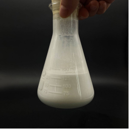
( Plasticiser)
Enabling High-Rise Building And Construction. In the race to construct greater, our plasticisers have actually been instrumental. They enable the manufacturing of self-compacting concrete (SCC), which streams easily right into complicated formwork and thick support cages without the need for mechanical vibration. This has reinvented the building of mega-tall structures, lowering labor prices and ensuring best loan consolidation also in one of the most hard to reach areas. Without our innovation, the sleek, slender accounts of modern high-rise buildings would be structurally and financially unviable.
Preserving Heritage and Facilities. Longevity is the trademark of our influence. By lowering the water-cement proportion, our plasticisers create concrete with very low permeability. This serves as a guard versus chlorides, sulfates, and freeze-thaw cycles, substantially expanding the service life of bridges, tunnels, and aquatic structures. We are honored that our items play a crucial duty in safeguarding the huge public financial investments made in worldwide framework, guaranteeing safety and sustainability for future generations.
Driving Sustainability. Our contribution to the planet is gauged in carbon conserved. By enhancing workability, we allow for the reduction of concrete web content in blends without compromising strength. Because concrete manufacturing is a significant resource of international carbon dioxide emissions, our plasticisers directly add to greener building techniques. We are aiding the industry transition in the direction of a low-carbon future, one cubic meter at a time.
Future Vision: Smart Fluids for a Digital Age
As we seek to the horizon, our vision for the Plasticiser is just one of knowledge and adjustment. We see a future where these ingredients are not simply passive lubricants, yet energetic individuals in the treating procedure. We are pioneering the growth of rheology-modifying admixtures that react to shear rates in real-time, important for the arising field of 3D concrete printing.
The Period of Smart Concrete. We are investing heavily in study to develop “smart” plasticisers that can interact with the matrix. Imagine a particle that launches hydration inhibitors throughout transport and then activates instantaneously upon pumping. This degree of control will remove waste and allow for unmatched accuracy in building. In addition, we are checking out bio-based polymers to replace petrochemical feedstocks, intending to accomplish a totally renewable product within the next years.
Digital Combination. Our future additionally includes integrating our chemistry with digital construction tools. We are developing plasticisers that work with computerized application systems linked to Building Information Modeling (BIM) software program. This will allow for real-time modifications to the mix style based upon ecological data, guaranteeing ideal performance no matter climate condition. We are developing the bridge in between molecular scientific research and digital engineering.
TRUNNANO chief executive officer Roger Luo said:” We exist to understand the flow of progression. Our plasticisers transform the rigid into the resilient, empowering humanity to construct a stronger, much more sustainable globe.”

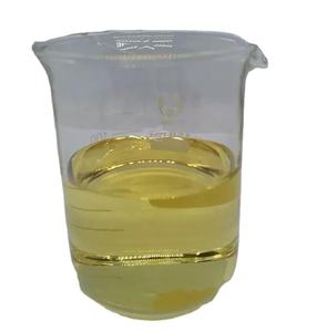
( Plasticiser)
Provider
Cabr-Concrete is a supplier under TRUNNANO of concrete fiber with over 12 years of experience in nano-building energy conservation and nanotechnology development. It accepts payment via Credit Card, T/T, West Union and Paypal. TRUNNANO will ship the goods to customers overseas through FedEx, DHL, by air, or by sea. If you are looking for admixture chemical, please feel free to contact us and send an inquiry.
Tags: polycarboxylate ether powder
All articles and pictures are from the Internet. If there are any copyright issues, please contact us in time to delete.
Inquiry us
Error: Contact form not found.