When engineers discuss materials that can make it through where steel melts and glass vaporizes, Silicon Carbide ceramics are often at the top of the checklist. This is not an unknown research laboratory interest; it is a material that silently powers industries, from the semiconductors in your phone to the brake discs in high-speed trains. What makes Silicon Carbide porcelains so amazing is not simply a list of residential properties, yet a mix of severe firmness, high thermal conductivity, and surprising chemical strength. In this write-up, we will explore the science behind these high qualities, the ingenuity of the production procedures, and the wide range of applications that have made Silicon Carbide porcelains a foundation of contemporary high-performance design
1. The Atomic Architecture of Toughness
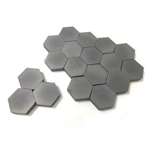
(Silicon Carbide Ceramics)
To recognize why Silicon Carbide ceramics are so hard, we need to begin with their atomic framework. Silicon carbide is a compound of silicon and carbon, set up in a lattice where each atom is tightly bound to four next-door neighbors in a tetrahedral geometry. This three-dimensional network of strong covalent bonds offers the product its hallmark buildings: high firmness, high melting point, and resistance to deformation. Unlike steels, which have cost-free electrons to lug both electrical power and warm, Silicon Carbide is a semiconductor. Its electrons are more snugly bound, which indicates it can perform electrical energy under specific problems yet continues to be an outstanding thermal conductor through vibrations of the crystal latticework, referred to as phonons
One of the most fascinating aspects of Silicon Carbide porcelains is their polymorphism. The same standard chemical structure can take shape into many different frameworks, referred to as polytypes, which vary just in the stacking series of their atomic layers. The most typical polytypes are 3C-SiC, 4H-SiC, and 6H-SiC, each with somewhat different digital and thermal homes. This adaptability allows products scientists to choose the ideal polytype for a specific application, whether it is for high-power electronics, high-temperature architectural components, or optical devices
One more key attribute of Silicon Carbide porcelains is their strong covalent bonding, which causes a high elastic modulus. This suggests that the product is extremely rigid and resists bending or extending under tons. At the very same time, Silicon Carbide ceramics display excellent flexural strength, often getting to numerous hundred megapascals. This combination of tightness and stamina makes them ideal for applications where dimensional stability is vital, such as in precision machinery or aerospace parts
2. The Alchemy of Production
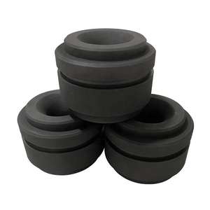
Creating a Silicon Carbide ceramic element is not as straightforward as baking clay in a kiln. The process begins with the manufacturing of high-purity Silicon Carbide powder, which can be synthesized with various methods, including the Acheson procedure, chemical vapor deposition, or laser-assisted synthesis. Each technique has its advantages and constraints, however the goal is constantly to produce a powder with the best fragment size, form, and purity for the desired application
When the powder is prepared, the following step is densification. This is where the actual difficulty exists, as the solid covalent bonds in Silicon Carbide make it challenging for the fragments to relocate and compact. To conquer this, manufacturers use a range of strategies, such as pressureless sintering, warm pressing, or stimulate plasma sintering. In pressureless sintering, the powder is warmed in a heater to a heat in the existence of a sintering help, which assists to decrease the activation energy for densification. Hot pressing, on the other hand, applies both warm and pressure to the powder, permitting faster and a lot more full densification at reduced temperatures
An additional innovative method is the use of additive manufacturing, or 3D printing, to develop intricate Silicon Carbide ceramic parts. Strategies like digital light processing (DLP) and stereolithography permit the accurate control of the shape and size of the final product. In DLP, a photosensitive material consisting of Silicon Carbide powder is healed by direct exposure to light, layer by layer, to develop the desired shape. The printed component is then sintered at heat to get rid of the material and densify the ceramic. This method opens new possibilities for the manufacturing of complex components that would certainly be tough or difficult to make using conventional approaches
3. The Many Faces of Silicon Carbide Ceramics
The one-of-a-kind homes of Silicon Carbide ceramics make them appropriate for a wide variety of applications, from daily customer items to sophisticated modern technologies. In the semiconductor industry, Silicon Carbide is utilized as a substratum material for high-power electronic devices, such as Schottky diodes and MOSFETs. These tools can run at higher voltages, temperature levels, and regularities than conventional silicon-based gadgets, making them optimal for applications in electrical lorries, renewable energy systems, and clever grids
In the field of aerospace, Silicon Carbide porcelains are utilized in components that have to stand up to extreme temperature levels and mechanical anxiety. For instance, Silicon Carbide fiber-reinforced Silicon Carbide matrix compounds (SiC/SiC CMCs) are being established for use in jet engines and hypersonic lorries. These materials can run at temperatures surpassing 1200 levels celsius, providing significant weight cost savings and improved efficiency over traditional nickel-based superalloys
Silicon Carbide porcelains likewise play a vital function in the manufacturing of high-temperature furnaces and kilns. Their high thermal conductivity and resistance to thermal shock make them optimal for components such as heating elements, crucibles, and furnace furniture. In the chemical handling market, Silicon Carbide ceramics are made use of in equipment that must stand up to rust and wear, such as pumps, shutoffs, and warm exchanger tubes. Their chemical inertness and high hardness make them perfect for handling aggressive media, such as liquified steels, acids, and alkalis
4. The Future of Silicon Carbide Ceramics
As research and development in products scientific research continue to advance, the future of Silicon Carbide ceramics looks appealing. New manufacturing methods, such as additive manufacturing and nanotechnology, are opening up new opportunities for the manufacturing of complicated and high-performance parts. At the exact same time, the growing demand for energy-efficient and high-performance innovations is driving the adoption of Silicon Carbide porcelains in a wide range of industries
One location of particular passion is the advancement of Silicon Carbide ceramics for quantum computing and quantum noticing. Specific polytypes of Silicon Carbide host defects that can function as quantum bits, or qubits, which can be manipulated at area temperature. This makes Silicon Carbide an encouraging platform for the development of scalable and functional quantum modern technologies
An additional amazing growth is the use of Silicon Carbide ceramics in lasting energy systems. For instance, Silicon Carbide porcelains are being utilized in the manufacturing of high-efficiency solar batteries and fuel cells, where their high thermal conductivity and chemical security can boost the performance and durability of these gadgets. As the globe continues to relocate in the direction of a more sustainable future, Silicon Carbide porcelains are most likely to play a significantly important role
5. Final thought: A Product for the Ages
( Silicon Carbide Ceramics)
Finally, Silicon Carbide ceramics are a remarkable class of materials that integrate severe solidity, high thermal conductivity, and chemical durability. Their special properties make them perfect for a vast array of applications, from everyday customer items to cutting-edge technologies. As research and development in products scientific research remain to development, the future of Silicon Carbide ceramics looks appealing, with new manufacturing strategies and applications arising all the time. Whether you are an engineer, a scientist, or just a person that appreciates the marvels of contemporary products, Silicon Carbide ceramics are sure to continue to impress and motivate
6. Supplier
Advanced Ceramics founded on October 17, 2012, is a high-tech enterprise committed to the research and development, production, processing, sales and technical services of ceramic relative materials and products. Our products includes but not limited to Boron Carbide Ceramic Products, Boron Nitride Ceramic Products, Silicon Carbide Ceramic Products, Silicon Nitride Ceramic Products, Zirconium Dioxide Ceramic Products, etc. If you are interested, please feel free to contact us.
Tags: Silicon Carbide Ceramics, Silicon Carbide Ceramic, Silicon Carbide
All articles and pictures are from the Internet. If there are any copyright issues, please contact us in time to delete.
Inquiry us
Error: Contact form not found.