1. Chemical Identification and Structural Diversity
1.1 Molecular Composition and Modulus Principle

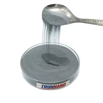
(Sodium Silicate Powder)
Sodium silicate, generally called water glass, is not a single compound yet a family of not natural polymers with the basic formula Na two O · nSiO two, where n represents the molar ratio of SiO two to Na two O– referred to as the “modulus.”
This modulus generally ranges from 1.6 to 3.8, seriously influencing solubility, thickness, alkalinity, and sensitivity.
Low-modulus silicates (n ≈ 1.6– 2.0) have more salt oxide, are extremely alkaline (pH > 12), and dissolve easily in water, developing thick, syrupy liquids.
High-modulus silicates (n ≈ 3.0– 3.8) are richer in silica, much less soluble, and usually look like gels or strong glasses that need heat or stress for dissolution.
In liquid option, salt silicate exists as a dynamic balance of monomeric silicate ions (e.g., SiO FOUR ⁴ ⁻), oligomers, and colloidal silica fragments, whose polymerization level increases with concentration and pH.
This architectural flexibility underpins its multifunctional roles throughout construction, manufacturing, and ecological design.
1.2 Manufacturing Methods and Business Kinds
Sodium silicate is industrially generated by merging high-purity quartz sand (SiO TWO) with soda ash (Na two CO ₃) in a furnace at 1300– 1400 ° C, generating a molten glass that is appeased and liquified in pressurized heavy steam or hot water.
The resulting fluid item is filtered, concentrated, and standardized to specific thickness (e.g., 1.3– 1.5 g/cm FIVE )and moduli for various applications.
It is additionally available as strong lumps, beads, or powders for storage stability and transport effectiveness, reconstituted on-site when required.
Worldwide manufacturing surpasses 5 million statistics tons each year, with major uses in detergents, adhesives, foundry binders, and– most considerably– building and construction products.
Quality control concentrates on SiO ₂/ Na two O ratio, iron web content (impacts color), and clarity, as contaminations can interfere with setting responses or catalytic efficiency.
(Sodium Silicate Powder)
2. Systems in Cementitious Solution
2.1 Alkali Activation and Early-Strength Development
In concrete modern technology, salt silicate serves as a vital activator in alkali-activated materials (AAMs), specifically when incorporated with aluminosilicate precursors like fly ash, slag, or metakaolin.
Its high alkalinity depolymerizes the silicate network of these SCMs, releasing Si ⁴ ⁺ and Al ³ ⁺ ions that recondense into a three-dimensional N-A-S-H (salt aluminosilicate hydrate) gel– the binding phase analogous to C-S-H in Rose city concrete.
When added directly to regular Portland concrete (OPC) blends, salt silicate accelerates very early hydration by raising pore service pH, promoting fast nucleation of calcium silicate hydrate and ettringite.
This causes dramatically lowered first and last setup times and enhanced compressive stamina within the first 1 day– valuable out of commission mortars, grouts, and cold-weather concreting.
Nonetheless, extreme dose can cause flash collection or efflorescence because of excess sodium moving to the surface area and responding with atmospheric CO ₂ to develop white sodium carbonate down payments.
Optimum dosing usually ranges from 2% to 5% by weight of concrete, calibrated via compatibility testing with regional products.
2.2 Pore Sealing and Surface Hardening
Water down salt silicate solutions are commonly used as concrete sealants and dustproofer treatments for industrial floorings, stockrooms, and parking frameworks.
Upon penetration right into the capillary pores, silicate ions react with complimentary calcium hydroxide (portlandite) in the concrete matrix to develop added C-S-H gel:
Ca( OH) ₂ + Na ₂ SiO SIX → CaSiO SIX · nH ₂ O + 2NaOH.
This response densifies the near-surface zone, decreasing leaks in the structure, enhancing abrasion resistance, and removing cleaning caused by weak, unbound fines.
Unlike film-forming sealers (e.g., epoxies or acrylics), salt silicate treatments are breathable, permitting moisture vapor transmission while blocking fluid ingress– crucial for avoiding spalling in freeze-thaw environments.
Multiple applications may be needed for extremely porous substratums, with curing durations between layers to enable full response.
Modern solutions frequently blend sodium silicate with lithium or potassium silicates to lessen efflorescence and boost long-term security.
3. Industrial Applications Beyond Building And Construction
3.1 Factory Binders and Refractory Adhesives
In metal casting, sodium silicate acts as a fast-setting, not natural binder for sand molds and cores.
When combined with silica sand, it develops a rigid structure that withstands liquified steel temperatures; CARBON MONOXIDE two gassing is frequently utilized to instantly cure the binder via carbonation:
Na Two SiO TWO + CARBON MONOXIDE TWO → SiO ₂ + Na Two CARBON MONOXIDE THREE.
This “CO two procedure” makes it possible for high dimensional precision and rapid mold turnaround, though residual salt carbonate can create casting defects otherwise appropriately vented.
In refractory cellular linings for heaters and kilns, sodium silicate binds fireclay or alumina accumulations, giving first eco-friendly stamina prior to high-temperature sintering establishes ceramic bonds.
Its affordable and convenience of usage make it vital in tiny factories and artisanal metalworking, despite competition from natural ester-cured systems.
3.2 Detergents, Catalysts, and Environmental Makes use of
As a building contractor in laundry and industrial detergents, sodium silicate buffers pH, protects against deterioration of washing maker components, and suspends dirt fragments.
It serves as a precursor for silica gel, molecular screens, and zeolites– products used in catalysis, gas separation, and water softening.
In environmental engineering, salt silicate is employed to stabilize infected soils with in-situ gelation, immobilizing hefty metals or radionuclides by encapsulation.
It likewise operates as a flocculant aid in wastewater treatment, enhancing the settling of suspended solids when integrated with metal salts.
Arising applications include fire-retardant coatings (forms protecting silica char upon heating) and passive fire defense for wood and textiles.
4. Security, Sustainability, and Future Outlook
4.1 Handling Considerations and Ecological Impact
Salt silicate solutions are strongly alkaline and can trigger skin and eye irritation; correct PPE– including handwear covers and safety glasses– is important throughout taking care of.
Spills should be neutralized with weak acids (e.g., vinegar) and contained to prevent dirt or river contamination, though the substance itself is safe and biodegradable with time.
Its primary environmental problem lies in raised sodium web content, which can affect soil structure and marine communities if launched in huge quantities.
Compared to artificial polymers or VOC-laden alternatives, sodium silicate has a reduced carbon impact, stemmed from plentiful minerals and calling for no petrochemical feedstocks.
Recycling of waste silicate options from commercial procedures is progressively practiced through precipitation and reuse as silica resources.
4.2 Advancements in Low-Carbon Construction
As the building industry seeks decarbonization, sodium silicate is main to the growth of alkali-activated concretes that eliminate or drastically minimize Rose city clinker– the source of 8% of global CO ₂ emissions.
Study concentrates on optimizing silicate modulus, combining it with choice activators (e.g., salt hydroxide or carbonate), and customizing rheology for 3D printing of geopolymer structures.
Nano-silicate diffusions are being checked out to improve early-age stamina without enhancing alkali material, alleviating lasting resilience threats like alkali-silica reaction (ASR).
Standardization efforts by ASTM, RILEM, and ISO aim to develop performance criteria and design guidelines for silicate-based binders, increasing their adoption in mainstream facilities.
In essence, sodium silicate exhibits exactly how an ancient material– made use of considering that the 19th century– remains to develop as a foundation of lasting, high-performance material science in the 21st century.
5. Supplier
TRUNNANO is a supplier of Sodium Silicate Powder, with over 12 years of experience in nano-building energy conservation and nanotechnology development. It accepts payment via Credit Card, T/T, West Union and Paypal. Trunnano will ship the goods to customers overseas through FedEx, DHL, by air, or by sea. If you want to know more about Sodium Silicate, please feel free to contact us and send an inquiry.
Tags: sodium silicate,sodium silicate water glass,sodium silicate liquid glass
All articles and pictures are from the Internet. If there are any copyright issues, please contact us in time to delete.
Inquiry us
Error: Contact form not found.