Concrete may appear simple– sand, rock, cement, water– but behind every smooth put and sturdy slab lies a covert choreography of molecules. In modern construction, managing that choreography means making use of wise additives. Amongst them, Polycarboxylate Superplasticizer Powder has actually ended up being a game-changer, letting designers dial in simply the appropriate fluidness without endangering stamina or durability. Much from being a simple comfort, this powder reshapes how concrete behaves, transforming stiff mixes right into flowing rivers of possibility and guaranteeing structures persevere for years. Its story blends scientific research, manufacturing skill, and real-world ingenuity in such a way that anybody curious regarding modern building can value.
1. Exactly How Molecules Unlock Concrete Fluidness
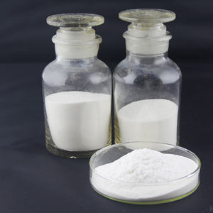
(Polycarboxylate Superplasticizer Powder)
Visualize attempting to mix honey with a spoon– that is what mixing concrete and water seems like without help. Concrete grains naturally clump with each other, capturing water inside their network and leaving little free wetness to lube circulation. Below, Polycarboxylate Superplasticizer Powder steps in with a brilliant molecular method. Once dissolved, its lengthy polymer chains extend external, physically avoiding bits from huddling as well close. These chains produce a shield called steric obstacle. Meanwhile, billed parts of the particle press fragments apart with electrostatic repulsion. With each other, these forces separate globs and release trapped water, making the mix fluid even when very little water is made use of.
The elegance of this system is precision. By changing the length and thickness of the polymer chains, manufacturers tailor just how highly the powder disperses particles and how much time the boosted circulation lasts. That indicates concrete can remain practical during lengthy distributions or tricky pours without rushing the crew. Due to the fact that the powder keeps its molecular behavior whether dry or liquified, individuals get flexibility in storage and taking care of while protecting efficiency.
2. From Laboratory Bench to Assembly Line
Making Polycarboxylate Superplasticizer Powder is component chemistry, part engineering art. It starts with synthesizing the polymer in fluid form, carefully managing response problems so the chains grow to the preferred size and style. Scientists select monomers that offer the right balance of water solubility, fee thickness, and chain flexibility. As soon as the polymer is developed, the challenge becomes turning it into a steady, free-flowing powder without weakening its efficiency.
This transformation normally includes spray drying out. The liquid polymer is atomized into tiny droplets that satisfy hot air, rapidly evaporating moisture and leaving great solid bits. Controlling temperature and air flow is essential– way too much warmth can harm the fragile polymer shape, while unequal drying develops clumps. Advanced plants monitor these parameters carefully, producing a powder that dissolves predictably and uniformly when mixed with water on website. The result is a product that retains the molecular knowledge made in the lab, prepared for global shipping and varied climates.
Packaging also matters. Since dampness can too soon activate the polymer, the powder is sealed in moisture-resistant containers, frequently with desiccants, so it gets to the jobsite specifically as planned. This focus to detail guarantees that the performance assured in the laboratory appears in the field, offering home builders self-confidence in every set.
3. Real World Power Across Construction Scenes
The effect of Polycarboxylate Superplasticizer Powder extends far past research laboratory curiosity. In ready-mix plants, it permits producers to reduced water content while keeping downturn, which means stronger concrete with much less concrete. Much less concrete not only cuts price but likewise decreases carbon footprint, lining up with sustainable building objectives. For precast backyards, the powder’s downturn retention is an advantage, allowing employees mold and mildew complicated forms over hours without consistent reworking.
Skyscraper construction gains from the powder’s capacity to produce self-compacting concrete. Such blends flow right into tight areas and around thick reinforcement without vibration, saving labor and improving surface high quality. In massive puts for bridges or foundations, extended workability prevents cool joints and makes certain consistent strength throughout. Even in extreme settings, like heat concreting, specialized grades of the powder maintain mixes plastic enough time to put appropriately.
Repair work and reconstruction projects also benefit. When patching old frameworks, professionals require mixes that bond well and stream into uneven spaces. The powder’s water-reducing power allows them utilize rich, sticky mortars that still relocate quickly right into location, decreasing the danger of weak points. This flexibility makes Polycarboxylate Superplasticizer Powder a relied on ally throughout the whole spectrum of concrete applications.
(Polycarboxylate Superplasticizer Powder)
4. Why Contractors Are Switching Over to the Powder Form
While fluid superplasticizers have actually been common for years, the powdered variant deals unique practical wins. Delivering liquids suggests much heavier tons, greater shipping expenses, and more stringent laws for spillage. Powders avoid these issues, reducing products weight and streamlining logistics, particularly for remote job websites or export markets. Storage space is simpler as well– no demand for unique tanks or issues about temperature-sensitive viscosity changes.
On site, employees just add the gauged powder to the mixer, where it disperses in water and triggers quickly. This simplicity speeds batching and decreases the possibility of dosing mistakes contrasted to managing thick liquids. For companies taking care of numerous tasks, the powder’s stability and service life imply they can stock reliable supplies without rapid turn over. The kind aspect also opens up doors to custom blending, where the powder can be combined with various other completely dry admixtures for tailored performance.
Another subtle benefit is dosage precision. Powders lend themselves to exact considering, aiding quality control teams hit specific efficiency targets batch after batch. This repeatability constructs trust fund with customers who require regular outcomes, from high-rise cores to highway overlays. In short, Polycarboxylate Superplasticizer Powder transforms an advanced chemical device right into an user-friendly property.
5. Balancing Efficiency with Practical Mindsets
Making Use Of Polycarboxylate Superplasticizer Powder sensibly needs understanding its interaction with other materials. Concrete type, extra cementitious materials like fly ash or slag, and also water high quality affect how the polymer does. Experienced formulators examination mixes to locate harmony– for instance, specific powders boost flow when blended with sedimentary rock powder, while others succeed with high-alumina cements.
Temperature plays a role too. Cold conditions sluggish dissolution, so staffs may pre-dissolve the powder in warm water or adjust blending time. On the other hand, very hot settings might call for specifically created powders that stand up to early adsorption onto cement fragments, maintaining slump. Home builders that realize these subtleties can exploit the powder’s complete potential as opposed to treat it as a one-size-fits-all remedy.
Educating matters. When teams know just how to blend, dose, and check the effects of Polycarboxylate Superplasticizer Powder, they avoid risks like overdosing, which can cause segregation, or underdosing, which leaves concrete extreme and unfeasible. With clear protocols and comments loopholes, the powder comes to be an accuracy tool in proficient hands.
(Polycarboxylate Superplasticizer Powder)
6. The Future Molded by Molecular Control
Building is moving toward smarter, greener methods, and Polycarboxylate Superplasticizer Powder fits normally right into that trajectory. Researchers continue improving polymer architectures to boost efficiency further– longer downturn retention, quicker establishing when required, or enhanced compatibility with brand-new binder systems like geopolymers. Some advances aim to make powders receptive to external triggers, such as temperature level or pH, using adaptive flow control during positioning.
Sustainability drives technology too. By making it possible for lower water and concrete use, the powder straight trims environmental effect. Paired with recycled accumulations and alternate binders, it assists create concrete that satisfies both structural and environmental demands. As digital batching systems advancement, accurate metering of the powder will certainly integrate effortlessly into automated plants, minimizing waste and increasing uniformity.
The recurring development suggests that Polycarboxylate Superplasticizer Powder will stay main to high-performance concrete. Its marital relationship of molecular class and sensible type ensures it can deal with tomorrow’s difficulties– taller towers, longer periods, and a lot more enthusiastic styles– without compromising quality or sustainability.
7. Making the Option Count
For concrete producers and professionals, picking the right Polycarboxylate Superplasticizer Powder is greater than picking a product; it is choosing a companion in efficiency. Factors like called for workability time, ambient problems, and mix layout need to line up with the powder’s characteristics. Dealing with providers that offer technical support and test information helps make certain success.
Evaluating little sets prior to major usage reveals communications distinct to a project’s products. Adjustments in dose or mixing method can after that be made confidently. In time, experience develops a data base that lets teams prepare for requirements and respond promptly, maintaining projects on schedule and on spec. In this way, the powder ends up being not simply an additive however a tactical device for affordable advantage.
8. Wrapping Circulation in Toughness
From its molecular roots to its existence on the jobsite, Polycarboxylate Superplasticizer Powder exemplifies how thoughtful chemistry fixes real-world problems. It approves fluidity without concession, simplifies logistics, and adapts to the varied needs of contemporary building. Its continued improvement promises even higher control over concrete’s habits, allowing home builders shape the developed setting with accuracy and self-confidence. In the dancing of fragments and polymers, this powder leads with intelligence, showing that the smallest ingredients can have the biggest influence.
9. Vendor
Cabr-Concrete is a supplier under TRUNNANO of Polycarboxylate Superplasticizer Powder with over 12 years of experience in nano-building energy conservation and nanotechnology development. It accepts payment via Credit Card, T/T, Western Union, and PayPal. TRUNNANO will ship the goods to customers overseas through FedEx, DHL, by air, or by sea. If you are looking for fosroc conplast wl, please feel free to contact us and send an inquiry.
Tags: polycarboxylate ether powder, polycarboxylate superplasticizer, superplasticizer powder
All articles and pictures are from the Internet. If there are any copyright issues, please contact us in time to delete.
Inquiry us
Error: Contact form not found.