Intro: The Crucible of Production
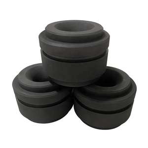
In the world of products science, where the alchemy of warmth changes base elements right into the foundation of world, there exists a vessel that stands as the sentinel of pureness. The Alumina Porcelain Crucible is not merely a container; it is the guardian of the liquified state, the quiet witness to the birth of semiconductors, superalloys, and the rarest earths. For centuries, humankind has actually battled to consist of fire, usually losing the fight as metal corroded the clay or warm shattered the vessel. We saw a globe limited by the delicacy of its devices, where the quest of high-temperature processing was shackled by the concern of contamination. This is the story of just how we took advantage of the crystalline structure of nature to redefine the limits of thermal endurance. We stand at the lead of refractory innovation, where the manipulation of aluminum oxide determines the efficiency of smelting and the durability of commercial cycles. Our brand was born from the understanding that the solution to extreme heat did not hinge on thicker walls, but in the pureness of the atomic lattice. We sought to introduce strength to the snake pit, verifying that by improving the ceramic bond, we might develop a future where temperature is no more an obstacle to technology. This is the story of control, pureness, and the fragile balance needed to hold the sunlight in our hands. It is a testimony to the power of ceramics to fix the thermal issues of deep space.

(Alumina Ceramic Crucible)
Brand Beginning: The Alchemist’s Problem
Our story begins not in an excellent laboratory, however in the disorderly warm of very early commercial shops where the odor of molten metal was a constant reminder of the constraints of refractory materials. The owners were disillusioned by the standard techniques of crucible construction, where graphite eroded right into the thaw and silica seeped pollutants into the alloy. They recognized that the trick to purity stocked chemical inertness, however this developed a brand-new trouble: a material that can hold up against the heat yet ruined under thermal shock. The obstacle was to make a ceramic that was not just warmth immune, however impervious to the hostile nature of molten metals. This mystery became our obsession. We pulled back into the r & d center, driven by the belief that the answer stocked the mineral diamond. We were established to locate a product that was not just a container, yet a shield that protected the integrity of the melt. We understood that the future of high-temperature applications depended upon a crucible that might assure outright pureness.
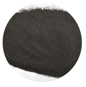
The Genesis of Purity. The early days were specified by unrelenting experimentation. Plenty of kiln cycles were run, and thousands of samples were ruined as we sought the excellent microstructure. We were looking for a density that might stop infiltration while preserving the strength to endure rapid heating. The advancement came when we transformed our interest to the particle size circulation of our basic materials. We recognized that by managing the fines and the coarse fractions, we could accomplish a green density that translated into a completely dense fired body. It was a Eureka minute that permitted us to develop a crucible that worked not just externally, but within the really pores of the ceramic. We had actually fractured the code of thermal shock resistance, verifying that by controlling the grain borders, we could attain higher stamina. This exploration marked the birth of our brand, a brand name committed to redefining the really significance of high-temperature containment.
Core Process: Forging the Fire
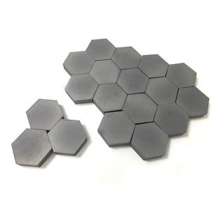
The development of our Alumina Ceramic Crucible is not a matter of molding and firing; it is a precise orchestration of basic material option and thermal profiling. It is a process that requires outright control, where the size of a grain or the rate of air conditioning can imply the distinction in between a high-performance crucible and a useless lump of clay. We do not make products; we craft options at the microstructural level. We resource the highest possible purity alumina powders, guaranteeing that every fragment is free from iron and silica impurities that could leach right into the thaw. Our proprietary mixing process guarantees an uniform mixture that assures constant performance throughout the crucible wall surface. We make use of innovative forming methods, consisting of isostatic pushing and slide casting, to accomplish the facility geometries required by our clients without compromising the thickness of the product. Whether we are creating a little laboratory crucible or a substantial industrial vessel, every shape is monitored with armed forces accuracy. Stress, dwell time, and mold launch are regulated to ensure uniformity. When the creating is full, the environment-friendly ware is dried and subjected to a shooting cycle that is the heart of our procedure. We utilize high-temperature kilns that get to over 1600 degrees Celsius, where the alumina particles undergo sintering to develop a solid, monolithic structure. This shooting account is a very closely guarded key, developed over years of experimentation. It guarantees that the end product has the optimal equilibrium of thickness, toughness, and thermal conductivity. Every crucible is then based on rigorous quality control tests. We gauge the dimensional accuracy, the density, and the chemical structure. Just when a crucible passes every single test does it earn the right to birth our logo. This commitment to quality ensures that when an engineer puts their valuable melt into our crucible, they are placing it into a vessel of outright integrity.
The Science of Inertness. At the heart of our innovation lies the concept of chemical stability. The molecular structure of aluminum oxide is inherently immune to response with most liquified steels and slags. Our engineers adjust the shooting ambience to make certain that the grain limits are devoid of glazed stages that could serve as a change. It is this specific adjustment of the ceramic matrix that gives our Alumina Porcelain Crucible its capability to resist deterioration and disintegration. We do not simply produce vessels; we produce a guard of atoms.

( Alumina Ceramic Crucible)
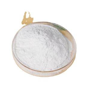
Accuracy Engineering and Quality Assurance. The production procedure starts with the mindful selection of high-purity alumina hydrate. This undergoes a collection of calcination steps to remove the chemically bound water and convert it to alpha alumina. We make use of innovative milling techniques to attain the desired particle size circulation. We after that include exclusive binders and dispersants to create a slurry that flows completely into our molds. As soon as the forming is total, the eco-friendly ware is dried out gradually to prevent breaking. The shooting cycle is one of the most critical action. We utilize a controlled ramping routine that permits the binders to wear out gradually without creating inner stresses. The optimal temperature is held for a details time to make certain full sintering. When cooled down, the crucibles are checked for any kind of surface defects. We then perform non-destructive screening, consisting of ultrasound scans, to guarantee there are no internal spaces or laminations. Just the best crucibles are chosen for delivery. This degree of examination makes certain that our item meets the greatest criteria of reliability.
The Art of Application. We recognize that an Alumina Ceramic Crucible is not just utilized for melting steels. It is a functional vessel that discovers application in crystal development, glass processing, and also nuclear research study. As a result, our core procedure includes a layer of application engineering. We function very closely with our clients to understand their certain needs, whether it is for high-temperature bearings or conductive polymers. We after that customize the surface finish of our crucible to ensure ideal release of the thaw. This bespoke strategy permits us to provide a remedy that is perfectly tailored to the job handy, ensuring optimum performance despite the outside variables. It is this level of service that sets us aside from the common crucibles discovered in the market.
Global Effect: The Silent Enabler
The impact of our Alumina Porcelain Crucible expands much beyond the research laboratory. It is installed in the heaters of the world’s most innovative production facilities and the reactors of advanced research establishments. We are the quiet enablers of development, allowing industries to press the borders of what is feasible. From the semiconductor field to the aerospace industry, our product is the undetectable hand that maintains the globe moving forward. We are pleased to be a part of the framework that powers the worldwide economic climate, ensuring that the products that build our globe are refined with miraculous pureness and efficiency.
Empowering Hefty Market. In the ruthless atmosphere of heavy equipment and industrial smelting, our Alumina Porcelain Crucible is the difference between a successful put and a disastrous failing. It is used in the melting of precious metals, the processing of uncommon planets, and the manufacturing of high-purity glass. By standing up to thermal shock and chemical attack, we extend the life expectancy of important processing devices, conserving markets countless dollars in upkeep and downtime. We are pleased to be a component of the heavy industry sector, aiding to build the facilities that powers the modern globe. Our crucibles are the workhorses of market, guaranteeing that the metals we rely on are produced effectively and securely.
Revolutionizing Electronics. Past metallurgy, our Alumina Ceramic Crucible is making waves in the electronics sector. As the demand for high-purity semiconductors grows, so does the requirement for crucibles that can hold up against the aggressive changes utilized in crystal growth. Our high-purity crucibles are the structure for these advanced applications, allowing researchers and engineers to expand crystals that are without flaws. We go to the center of the electronics change, confirming that our item is not just a container, yet an important part in the production of the chips that power our digital lives.
Driving Sustainability. Our payment to the planet is measured in power saved and waste decreased. By supplying a crucible that lasts longer and needs much less regular replacement, we aid to reduce the ecological footprint of commercial handling. We are honored to be a component of the eco-friendly innovation movement, assisting sectors to come to be more lasting and effective. Our team believe that by making processing vessels that are stronger and extra resilient, we can help to build a cleaner, greener future for all. We are dedicated to reducing our own carbon impact with energy-efficient manufacturing processes and the advancement of recyclable refractory materials.
Future Vision: The Age of Smart Refractories

( Alumina Ceramic Crucible)
As we aim to the horizon, our vision for the Alumina Porcelain Crucible is just one of knowledge and combination. We see a future where these ceramic vessels are not just easy containers, but energetic individuals in the melting process. We are pioneering the advancement of crucibles with embedded sensing units that can check the temperature level and chemistry of the melt in real-time. We are spending greatly in research study to produce nano-composites that incorporate the thermal security of alumina with the durability of zirconia. This will create materials that are not simply heat resistant, yet virtually unbreakable. In addition, we are discovering making use of additive production to create complex interior geometries that maximize warmth transfer and fluid characteristics within the crucible. By utilizing 3D printing innovation, we intend to significantly minimize the lead time for customized crucible designs, permitting our clients to introduce much faster. We are constructing the bridge between traditional ceramics and advanced products scientific research, making certain that our crucibles stay the vessel of selection for the markets of tomorrow.
TRUNNANO CEO Roger Luo said:”We exist to understand the warm of development. Our Alumina Porcelain Crucible changes molten turmoil right into pure possibility, empowering humankind to build a brighter and advanced world.”
Vendor
Alumina Technology Co., Ltd focus on the research and development, production and sales of aluminum oxide powder, aluminum oxide products, aluminum oxide crucible, etc., serving the electronics, ceramics, chemical and other industries. Since its establishment in 2005, the company has been committed to providing customers with the best products and services. If you are looking for high quality alpha alumina, please feel free to contact us.
Tags: Alumina Ceramic Crucible, Alumina Ceramic, Ceramic Crucible
All articles and pictures are from the Internet. If there are any copyright issues, please contact us in time to delete.
Inquiry us
Error: Contact form not found.