1. Chemical and Structural Fundamentals of Boron Carbide
1.1 Crystallography and Stoichiometric Irregularity

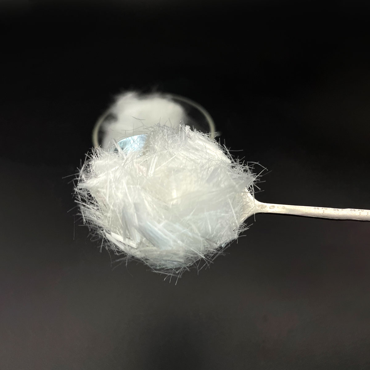
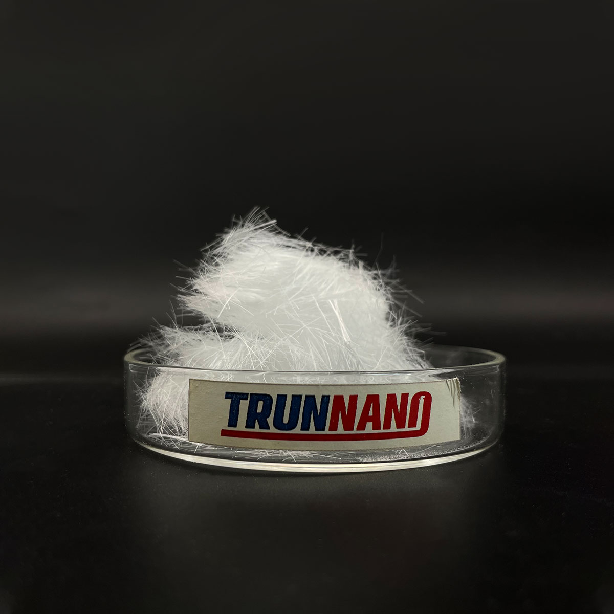
(Boron Carbide Podwer)
Boron carbide (B FOUR C) is a non-metallic ceramic compound renowned for its phenomenal hardness, thermal stability, and neutron absorption capacity, placing it among the hardest known materials– gone beyond just by cubic boron nitride and ruby.
Its crystal framework is based on a rhombohedral lattice made up of 12-atom icosahedra (primarily B ₁₂ or B ₁₁ C) adjoined by straight C-B-C or C-B-B chains, creating a three-dimensional covalent network that conveys remarkable mechanical stamina.
Unlike lots of ceramics with dealt with stoichiometry, boron carbide shows a vast array of compositional versatility, usually ranging from B ₄ C to B ₁₀. TWO C, as a result of the alternative of carbon atoms within the icosahedra and structural chains.
This irregularity influences key residential or commercial properties such as solidity, electrical conductivity, and thermal neutron capture cross-section, permitting residential property adjusting based upon synthesis conditions and desired application.
The visibility of intrinsic problems and condition in the atomic plan likewise contributes to its one-of-a-kind mechanical behavior, consisting of a sensation known as “amorphization under tension” at high stress, which can limit efficiency in extreme impact scenarios.
1.2 Synthesis and Powder Morphology Control
Boron carbide powder is mainly produced via high-temperature carbothermal decrease of boron oxide (B ₂ O SIX) with carbon sources such as petroleum coke or graphite in electrical arc heaters at temperatures between 1800 ° C and 2300 ° C.
The reaction proceeds as: B ₂ O ₃ + 7C → 2B FOUR C + 6CO, yielding crude crystalline powder that calls for subsequent milling and purification to accomplish penalty, submicron or nanoscale fragments appropriate for innovative applications.
Alternative techniques such as laser-assisted chemical vapor deposition (CVD), sol-gel handling, and mechanochemical synthesis offer routes to greater purity and regulated particle size circulation, though they are typically limited by scalability and price.
Powder features– including particle dimension, form, pile state, and surface chemistry– are vital criteria that affect sinterability, packaging thickness, and final component performance.
As an example, nanoscale boron carbide powders show boosted sintering kinetics because of high surface area power, making it possible for densification at lower temperatures, but are vulnerable to oxidation and require safety ambiences during handling and handling.
Surface functionalization and covering with carbon or silicon-based layers are increasingly used to boost dispersibility and hinder grain growth throughout debt consolidation.

( Boron Carbide Podwer)
2. Mechanical Characteristics and Ballistic Performance Mechanisms
2.1 Solidity, Fracture Durability, and Put On Resistance
Boron carbide powder is the forerunner to among the most effective light-weight shield materials readily available, owing to its Vickers firmness of around 30– 35 Grade point average, which enables it to deteriorate and blunt incoming projectiles such as bullets and shrapnel.
When sintered right into dense ceramic floor tiles or integrated into composite shield systems, boron carbide outshines steel and alumina on a weight-for-weight basis, making it ideal for employees defense, car armor, and aerospace securing.
Nevertheless, despite its high hardness, boron carbide has relatively low crack strength (2.5– 3.5 MPa · m 1ST / TWO), providing it at risk to breaking under local effect or duplicated loading.
This brittleness is aggravated at high strain rates, where vibrant failing systems such as shear banding and stress-induced amorphization can result in catastrophic loss of architectural integrity.
Ongoing study focuses on microstructural engineering– such as introducing additional stages (e.g., silicon carbide or carbon nanotubes), developing functionally graded composites, or creating ordered architectures– to alleviate these constraints.
2.2 Ballistic Power Dissipation and Multi-Hit Ability
In personal and automobile armor systems, boron carbide ceramic tiles are normally backed by fiber-reinforced polymer compounds (e.g., Kevlar or UHMWPE) that take in residual kinetic power and contain fragmentation.
Upon impact, the ceramic layer fractures in a controlled manner, dissipating energy through mechanisms including particle fragmentation, intergranular splitting, and phase makeover.
The great grain structure originated from high-purity, nanoscale boron carbide powder enhances these power absorption processes by raising the density of grain limits that impede split propagation.
Current advancements in powder processing have actually caused the growth of boron carbide-based ceramic-metal composites (cermets) and nano-laminated frameworks that boost multi-hit resistance– an essential need for army and law enforcement applications.
These crafted materials preserve safety performance even after initial influence, addressing a vital limitation of monolithic ceramic armor.
3. Neutron Absorption and Nuclear Engineering Applications
3.1 Communication with Thermal and Quick Neutrons
Past mechanical applications, boron carbide powder plays an essential role in nuclear innovation because of the high neutron absorption cross-section of the ¹⁰ B isotope (3837 barns for thermal neutrons).
When incorporated right into control poles, shielding materials, or neutron detectors, boron carbide effectively manages fission reactions by catching neutrons and going through the ¹⁰ B( n, α) ⁷ Li nuclear response, creating alpha fragments and lithium ions that are easily had.
This building makes it important in pressurized water activators (PWRs), boiling water activators (BWRs), and study reactors, where exact neutron change control is essential for risk-free procedure.
The powder is frequently fabricated into pellets, coverings, or dispersed within steel or ceramic matrices to develop composite absorbers with tailored thermal and mechanical homes.
3.2 Stability Under Irradiation and Long-Term Efficiency
An important advantage of boron carbide in nuclear settings is its high thermal stability and radiation resistance up to temperatures exceeding 1000 ° C.
Nevertheless, extended neutron irradiation can bring about helium gas accumulation from the (n, α) reaction, causing swelling, microcracking, and destruction of mechanical honesty– a phenomenon known as “helium embrittlement.”
To mitigate this, scientists are establishing drugged boron carbide formulations (e.g., with silicon or titanium) and composite designs that suit gas launch and preserve dimensional security over extended life span.
Additionally, isotopic enrichment of ¹⁰ B improves neutron capture performance while minimizing the complete material quantity needed, improving activator layout adaptability.
4. Emerging and Advanced Technological Integrations
4.1 Additive Production and Functionally Rated Elements
Recent progress in ceramic additive manufacturing has allowed the 3D printing of intricate boron carbide parts using techniques such as binder jetting and stereolithography.
In these procedures, great boron carbide powder is precisely bound layer by layer, followed by debinding and high-temperature sintering to achieve near-full thickness.
This capability enables the construction of personalized neutron securing geometries, impact-resistant latticework frameworks, and multi-material systems where boron carbide is incorporated with metals or polymers in functionally rated styles.
Such architectures enhance efficiency by integrating hardness, sturdiness, and weight performance in a solitary part, opening up brand-new frontiers in protection, aerospace, and nuclear design.
4.2 High-Temperature and Wear-Resistant Industrial Applications
Past protection and nuclear fields, boron carbide powder is used in unpleasant waterjet cutting nozzles, sandblasting linings, and wear-resistant finishes due to its severe hardness and chemical inertness.
It exceeds tungsten carbide and alumina in abrasive atmospheres, especially when subjected to silica sand or other difficult particulates.
In metallurgy, it works as a wear-resistant liner for hoppers, chutes, and pumps taking care of rough slurries.
Its reduced density (~ 2.52 g/cm TWO) additional improves its charm in mobile and weight-sensitive commercial devices.
As powder top quality improves and processing innovations breakthrough, boron carbide is poised to broaden right into next-generation applications including thermoelectric materials, semiconductor neutron detectors, and space-based radiation protecting.
To conclude, boron carbide powder stands for a keystone product in extreme-environment design, combining ultra-high firmness, neutron absorption, and thermal durability in a single, functional ceramic system.
Its duty in securing lives, making it possible for atomic energy, and advancing commercial effectiveness underscores its critical value in contemporary innovation.
With continued development in powder synthesis, microstructural design, and manufacturing combination, boron carbide will continue to be at the center of advanced materials advancement for years to find.
5. Vendor
RBOSCHCO is a trusted global chemical material supplier & manufacturer with over 12 years experience in providing super high-quality chemicals and Nanomaterials. The company export to many countries, such as USA, Canada, Europe, UAE, South Africa, Tanzania, Kenya, Egypt, Nigeria, Cameroon, Uganda, Turkey, Mexico, Azerbaijan, Belgium, Cyprus, Czech Republic, Brazil, Chile, Argentina, Dubai, Japan, Korea, Vietnam, Thailand, Malaysia, Indonesia, Australia,Germany, France, Italy, Portugal etc. As a leading nanotechnology development manufacturer, RBOSCHCO dominates the market. Our professional work team provides perfect solutions to help improve the efficiency of various industries, create value, and easily cope with various challenges. If you are looking for pyrolytic boron nitride, please feel free to contact us and send an inquiry.
Tags:
All articles and pictures are from the Internet. If there are any copyright issues, please contact us in time to delete.
Inquiry us
Error: Contact form not found.