1. Material Fundamentals and Microstructural Qualities of Alumina Ceramics
1.1 Composition, Purity Qualities, and Crystallographic Properties

(Alumina Ceramic Wear Liners)
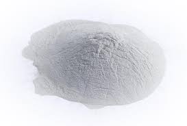
Alumina (Al Two O THREE), or aluminum oxide, is one of the most extensively made use of technical ceramics in industrial design due to its excellent balance of mechanical strength, chemical security, and cost-effectiveness.
When crafted right into wear liners, alumina porcelains are generally fabricated with purity degrees ranging from 85% to 99.9%, with higher pureness corresponding to boosted solidity, wear resistance, and thermal performance.
The dominant crystalline stage is alpha-alumina, which embraces a hexagonal close-packed (HCP) framework characterized by strong ionic and covalent bonding, adding to its high melting point (~ 2072 ° C )and low thermal conductivity.
Microstructurally, alumina ceramics contain fine, equiaxed grains whose dimension and distribution are regulated during sintering to optimize mechanical homes.
Grain dimensions generally range from submicron to a number of micrometers, with better grains generally boosting fracture toughness and resistance to split propagation under abrasive filling.
Small ingredients such as magnesium oxide (MgO) are commonly presented in trace total up to hinder abnormal grain growth throughout high-temperature sintering, guaranteeing consistent microstructure and dimensional stability.
The resulting product displays a Vickers solidity of 1500– 2000 HV, dramatically exceeding that of solidified steel (generally 600– 800 HV), making it exceptionally immune to surface deterioration in high-wear settings.
1.2 Mechanical and Thermal Performance in Industrial Conditions
Alumina ceramic wear liners are chosen largely for their outstanding resistance to abrasive, erosive, and sliding wear mechanisms widespread in bulk material dealing with systems.
They possess high compressive toughness (up to 3000 MPa), excellent flexural stamina (300– 500 MPa), and superb stiffness (Youthful’s modulus of ~ 380 Grade point average), allowing them to stand up to intense mechanical loading without plastic contortion.
Although inherently fragile contrasted to steels, their low coefficient of friction and high surface hardness decrease fragment attachment and decrease wear prices by orders of magnitude relative to steel or polymer-based choices.
Thermally, alumina preserves architectural honesty approximately 1600 ° C in oxidizing ambiences, permitting use in high-temperature handling settings such as kiln feed systems, central heating boiler ducting, and pyroprocessing equipment.

( Alumina Ceramic Wear Liners)
Its low thermal expansion coefficient (~ 8 × 10 ⁻⁶/ K) adds to dimensional stability throughout thermal cycling, decreasing the danger of cracking as a result of thermal shock when effectively mounted.
Additionally, alumina is electrically insulating and chemically inert to many acids, alkalis, and solvents, making it suitable for harsh atmospheres where metallic linings would weaken rapidly.
These consolidated homes make alumina porcelains ideal for safeguarding crucial framework in mining, power generation, cement production, and chemical handling industries.
2. Production Processes and Layout Integration Methods
2.1 Forming, Sintering, and Quality Assurance Protocols
The manufacturing of alumina ceramic wear liners includes a sequence of precision production actions made to attain high thickness, very little porosity, and regular mechanical efficiency.
Raw alumina powders are refined through milling, granulation, and creating techniques such as dry pushing, isostatic pressing, or extrusion, depending upon the preferred geometry– tiles, plates, pipelines, or custom-shaped segments.
Green bodies are after that sintered at temperature levels between 1500 ° C and 1700 ° C in air, advertising densification with solid-state diffusion and achieving loved one densities exceeding 95%, usually approaching 99% of theoretical thickness.
Complete densification is essential, as residual porosity works as stress and anxiety concentrators and increases wear and fracture under service problems.
Post-sintering procedures may consist of diamond grinding or lapping to accomplish tight dimensional resistances and smooth surface finishes that decrease friction and bit trapping.
Each set goes through strenuous quality assurance, consisting of X-ray diffraction (XRD) for stage evaluation, scanning electron microscopy (SEM) for microstructural assessment, and firmness and bend testing to verify conformity with global requirements such as ISO 6474 or ASTM B407.
2.2 Placing Techniques and System Compatibility Considerations
Reliable assimilation of alumina wear linings right into industrial equipment calls for mindful interest to mechanical accessory and thermal growth compatibility.
Common setup methods include sticky bonding utilizing high-strength ceramic epoxies, mechanical attaching with studs or anchors, and embedding within castable refractory matrices.
Glue bonding is commonly used for level or delicately rounded surfaces, offering consistent stress and anxiety circulation and vibration damping, while stud-mounted systems allow for simple replacement and are favored in high-impact areas.
To suit differential thermal development in between alumina and metallic substrates (e.g., carbon steel), engineered gaps, adaptable adhesives, or compliant underlayers are integrated to prevent delamination or cracking during thermal transients.
Designers should likewise consider side defense, as ceramic tiles are at risk to damaging at subjected edges; options consist of diagonal sides, steel shadows, or overlapping tile arrangements.
Appropriate installation makes certain lengthy service life and takes full advantage of the protective function of the lining system.
3. Wear Mechanisms and Performance Evaluation in Solution Environments
3.1 Resistance to Abrasive, Erosive, and Influence Loading
Alumina ceramic wear linings master settings controlled by 3 key wear mechanisms: two-body abrasion, three-body abrasion, and particle erosion.
In two-body abrasion, tough particles or surfaces directly gouge the liner surface, a common occurrence in chutes, receptacles, and conveyor changes.
Three-body abrasion entails loose bits trapped in between the liner and relocating material, leading to rolling and damaging activity that progressively gets rid of product.
Abrasive wear occurs when high-velocity particles strike the surface area, especially in pneumatic conveying lines and cyclone separators.
As a result of its high solidity and reduced fracture strength, alumina is most reliable in low-impact, high-abrasion circumstances.
It carries out extremely well against siliceous ores, coal, fly ash, and cement clinker, where wear rates can be lowered by 10– 50 times contrasted to moderate steel linings.
However, in applications including duplicated high-energy effect, such as main crusher chambers, hybrid systems integrating alumina floor tiles with elastomeric supports or metal shields are often used to absorb shock and avoid fracture.
3.2 Field Testing, Life Cycle Analysis, and Failure Setting Assessment
Performance evaluation of alumina wear linings entails both research laboratory screening and field monitoring.
Standardized examinations such as the ASTM G65 dry sand rubber wheel abrasion examination provide comparative wear indices, while personalized slurry disintegration rigs imitate site-specific problems.
In industrial settings, use rate is normally measured in mm/year or g/kWh, with service life forecasts based upon first thickness and observed deterioration.
Failure settings consist of surface area polishing, micro-cracking, spalling at edges, and total floor tile dislodgement due to adhesive destruction or mechanical overload.
Source evaluation commonly exposes setup errors, incorrect quality selection, or unexpected impact lots as main contributors to premature failing.
Life cycle price analysis consistently shows that regardless of higher preliminary costs, alumina liners supply superior overall price of ownership because of prolonged replacement periods, reduced downtime, and reduced upkeep labor.
4. Industrial Applications and Future Technological Advancements
4.1 Sector-Specific Executions Across Heavy Industries
Alumina ceramic wear linings are deployed across a broad range of industrial fields where material deterioration positions functional and economic challenges.
In mining and mineral handling, they protect transfer chutes, mill linings, hydrocyclones, and slurry pumps from abrasive slurries consisting of quartz, hematite, and various other tough minerals.
In power plants, alumina floor tiles line coal pulverizer ducts, boiler ash hoppers, and electrostatic precipitator components revealed to fly ash erosion.
Concrete suppliers make use of alumina linings in raw mills, kiln inlet zones, and clinker conveyors to fight the very rough nature of cementitious products.
The steel market employs them in blast heating system feed systems and ladle shadows, where resistance to both abrasion and modest thermal loads is necessary.
Even in less traditional applications such as waste-to-energy plants and biomass handling systems, alumina porcelains supply long lasting security versus chemically hostile and fibrous materials.
4.2 Arising Patterns: Compound Systems, Smart Liners, and Sustainability
Existing study concentrates on enhancing the sturdiness and functionality of alumina wear systems through composite layout.
Alumina-zirconia (Al Two O FOUR-ZrO ₂) compounds take advantage of transformation toughening from zirconia to improve split resistance, while alumina-titanium carbide (Al ₂ O FOUR-TiC) qualities supply improved efficiency in high-temperature moving wear.
An additional innovation includes installing sensors within or below ceramic linings to check wear progression, temperature, and influence frequency– making it possible for predictive maintenance and digital twin combination.
From a sustainability viewpoint, the extensive service life of alumina liners minimizes product intake and waste generation, lining up with circular economy principles in industrial procedures.
Recycling of invested ceramic liners into refractory accumulations or building materials is likewise being discovered to lessen environmental impact.
In conclusion, alumina ceramic wear liners represent a keystone of contemporary commercial wear protection modern technology.
Their exceptional firmness, thermal security, and chemical inertness, combined with mature production and installation techniques, make them important in combating product degradation across hefty industries.
As material scientific research advancements and electronic tracking becomes extra integrated, the next generation of wise, resilient alumina-based systems will certainly additionally boost operational performance and sustainability in unpleasant environments.
Provider
Alumina Technology Co., Ltd focus on the research and development, production and sales of aluminum oxide powder, aluminum oxide products, aluminum oxide crucible, etc., serving the electronics, ceramics, chemical and other industries. Since its establishment in 2005, the company has been committed to providing customers with the best products and services. If you are looking for high quality 99 alumina, please feel free to contact us. (nanotrun@yahoo.com)
Tags: Alumina Ceramic Wear Liners, Alumina Ceramics, alumina
All articles and pictures are from the Internet. If there are any copyright issues, please contact us in time to delete.
Inquiry us
Error: Contact form not found.