Introduction: The Ubiquitous “User Interface Magicians”
Surfactants are the unseen heroes of modern sector and life, found all over from cleaning items to drugs, from oil removal to food processing. These one-of-a-kind chemicals serve as bridges between oil and water by changing the surface tension of fluids, coming to be indispensable practical ingredients in numerous industries. This write-up will offer an in-depth exploration of surfactants from a worldwide perspective, covering their definition, primary types, comprehensive applications, and the special features of each category, providing a thorough recommendation for industry experts and interested learners.
Scientific Meaning and Working Principles of Surfactants
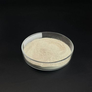
Surfactant, short for “Surface area Energetic Agent,” refers to a course of compounds that can substantially minimize the surface area stress of a liquid or the interfacial stress between 2 stages. These molecules possess an one-of-a-kind amphiphilic framework, consisting of a hydrophilic (water-loving) head and a hydrophobic (water-repelling, commonly lipophilic) tail. When surfactants are added to water, the hydrophobic tails try to run away the liquid setting, while the hydrophilic heads remain in contact with water, triggering the molecules to line up directionally at the interface.
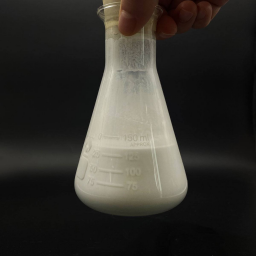
This positioning produces a number of essential results: decrease of surface area tension, promotion of emulsification, solubilization, wetting, and frothing. Above the vital micelle concentration (CMC), surfactants create micelles where their hydrophobic tails cluster inward and hydrophilic heads face external towards the water, thus encapsulating oily materials inside and enabling cleansing and emulsification features. The worldwide surfactant market reached about USD 43 billion in 2023 and is forecasted to expand to USD 58 billion by 2030, with a compound yearly growth rate (CAGR) of regarding 4.3%, mirroring their fundamental role in the international economic climate.
(Surfactants)
Key Types of Surfactants and International Category Requirements
The global classification of surfactants is commonly based upon the ionization features of their hydrophilic teams, a system widely recognized by the global scholastic and commercial neighborhoods. The following 4 groups stand for the industry-standard category:
Anionic Surfactants
Anionic surfactants bring an unfavorable fee on their hydrophilic group after ionization in water. They are the most produced and widely applied type internationally, representing regarding 50-60% of the total market share. Usual examples consist of:
Sulfonates: Such as Linear Alkylbenzene Sulfonates (LAS), the major component in washing cleaning agents
Sulfates: Such as Salt Dodecyl Sulfate (SDS), commonly used in personal treatment items
Carboxylates: Such as fatty acid salts found in soaps
Cationic Surfactants
Cationic surfactants carry a favorable cost on their hydrophilic team after ionization in water. This classification uses good anti-bacterial homes and fabric-softening capacities yet typically has weak cleaning power. Key applications consist of:
Four Ammonium Compounds: Made use of as anti-bacterials and fabric conditioners
Imidazoline Derivatives: Made use of in hair conditioners and individual care items
Zwitterionic (Amphoteric) Surfactants
Zwitterionic surfactants carry both positive and unfavorable charges, and their properties differ with pH. They are commonly mild and very compatible, extensively used in premium individual care items. Normal representatives include:
Betaines: Such as Cocamidopropyl Betaine, utilized in light hair shampoos and body cleans
Amino Acid By-products: Such as Alkyl Glutamates, made use of in premium skin care products
Nonionic Surfactants
Nonionic surfactants do not ionize in water; their hydrophilicity comes from polar teams such as ethylene oxide chains or hydroxyl groups. They are insensitive to difficult water, typically generate less foam, and are widely utilized in various commercial and durable goods. Main kinds include:
Polyoxyethylene Ethers: Such as Fatty Alcohol Ethoxylates, made use of for cleansing and emulsification
Alkylphenol Ethoxylates: Extensively used in industrial applications, yet their use is restricted due to ecological issues
Sugar-based Surfactants: Such as Alkyl Polyglucosides, stemmed from renewable resources with excellent biodegradability
( Surfactants)
Worldwide Point Of View on Surfactant Application Fields
Household and Personal Treatment Industry
This is the largest application location for surfactants, representing over 50% of global intake. The item variety extends from laundry detergents and dishwashing fluids to hair shampoos, body laundries, and toothpaste. Demand for mild, naturally-derived surfactants remains to grow in Europe and The United States And Canada, while the Asia-Pacific area, driven by population growth and boosting disposable income, is the fastest-growing market.
Industrial and Institutional Cleansing
Surfactants play an essential function in industrial cleansing, consisting of cleansing of food handling devices, car washing, and metal therapy. EU’s REACH policies and United States EPA standards impose rigorous guidelines on surfactant selection in these applications, driving the development of more environmentally friendly options.
Petroleum Removal and Boosted Oil Healing (EOR)
In the petroleum sector, surfactants are utilized for Boosted Oil Recovery (EOR) by minimizing the interfacial stress between oil and water, aiding to release recurring oil from rock formations. This innovation is widely made use of in oil areas between East, North America, and Latin America, making it a high-value application location for surfactants.
Farming and Pesticide Formulations
Surfactants function as adjuvants in pesticide formulas, boosting the spread, bond, and penetration of active components on plant surfaces. With expanding international focus on food protection and lasting farming, this application area continues to broaden, specifically in Asia and Africa.
Drugs and Biotechnology
In the pharmaceutical sector, surfactants are used in medication delivery systems to improve the bioavailability of improperly soluble medicines. During the COVID-19 pandemic, certain surfactants were utilized in some vaccination formulations to maintain lipid nanoparticles.
Food Industry
Food-grade surfactants serve as emulsifiers, stabilizers, and foaming representatives, commonly located in baked items, ice cream, delicious chocolate, and margarine. The Codex Alimentarius Compensation (CODEX) and nationwide regulative companies have stringent criteria for these applications.
Textile and Natural Leather Processing
Surfactants are utilized in the fabric industry for wetting, washing, dyeing, and finishing procedures, with substantial need from international fabric production centers such as China, India, and Bangladesh.
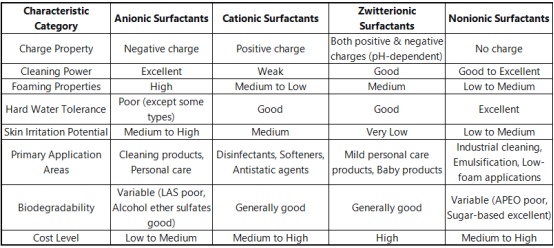
Contrast of Surfactant Types and Selection Guidelines
Choosing the appropriate surfactant calls for consideration of multiple elements, consisting of application needs, cost, environmental conditions, and regulatory demands. The following table summarizes the crucial qualities of the 4 main surfactant classifications:
( Comparison of Surfactant Types and Selection Guidelines)
Key Considerations for Selecting Surfactants:
HLB Worth (Hydrophilic-Lipophilic Equilibrium): Guides emulsifier option, ranging from 0 (entirely lipophilic) to 20 (entirely hydrophilic)
Ecological Compatibility: Includes biodegradability, ecotoxicity, and eco-friendly resources content
Regulative Compliance: Should stick to local regulations such as EU REACH and United States TSCA
Efficiency Demands: Such as cleansing performance, lathering features, viscosity modulation
Cost-Effectiveness: Balancing efficiency with complete formulation cost
Supply Chain Stability: Influence of worldwide occasions (e.g., pandemics, disputes) on resources supply
International Trends and Future Expectation
Presently, the global surfactant market is greatly affected by sustainable advancement principles, regional market demand distinctions, and technical development, exhibiting a diversified and vibrant transformative course. In regards to sustainability and green chemistry, the global trend is very clear: the sector is increasing its change from reliance on fossil fuels to the use of renewable energies. Bio-based surfactants, such as alkyl polysaccharides derived from coconut oil, hand kernel oil, or sugars, are experiencing proceeded market need growth as a result of their outstanding biodegradability and reduced carbon impact. Specifically in mature markets such as Europe and The United States and Canada, rigorous ecological regulations (such as the EU’s REACH policy and ecolabel qualification) and boosting consumer preference for “natural” and “eco-friendly” products are jointly driving formula upgrades and basic material alternative. This shift is not restricted to basic material sources but prolongs throughout the entire item lifecycle, including developing molecular frameworks that can be rapidly and entirely mineralized in the atmosphere, enhancing manufacturing procedures to decrease energy consumption and waste, and making much safer chemicals in accordance with the twelve concepts of eco-friendly chemistry.
From the viewpoint of local market attributes, different areas worldwide display unique development concentrates. As leaders in modern technology and guidelines, Europe and North America have the greatest needs for the sustainability, safety, and functional certification of surfactants, with premium personal care and home products being the main battlefield for innovation. The Asia-Pacific area, with its big populace, quick urbanization, and increasing middle class, has become the fastest-growing engine in the international surfactant market. Its demand currently concentrates on affordable remedies for fundamental cleaning and personal treatment, yet a trend in the direction of premium and green products is increasingly evident. Latin America and the Center East, on the other hand, are showing solid and specific demand in particular industrial industries, such as enhanced oil recuperation modern technologies in oil extraction and agricultural chemical adjuvants.
Looking in advance, technical technology will certainly be the core driving force for market development. R&D focus is strengthening in several crucial directions: first of all, establishing multifunctional surfactants, i.e., single-molecule frameworks having numerous residential or commercial properties such as cleansing, softening, and antistatic residential properties, to streamline formulas and boost performance; second of all, the rise of stimulus-responsive surfactants, these “smart” molecules that can respond to changes in the outside setting (such as particular pH worths, temperatures, or light), making it possible for exact applications in circumstances such as targeted drug release, regulated emulsification, or petroleum extraction. Third, the commercial possibility of biosurfactants is being more discovered. Rhamnolipids and sophorolipids, created by microbial fermentation, have broad application leads in environmental removal, high-value-added individual treatment, and farming as a result of their exceptional environmental compatibility and distinct properties. Ultimately, the cross-integration of surfactants and nanotechnology is opening up new possibilities for medication shipment systems, advanced materials preparation, and power storage.
( Surfactants)
Key Factors To Consider for Surfactant Selection
In useful applications, selecting the most suitable surfactant for a certain item or process is a complex systems design task that requires detailed factor to consider of numerous related factors. The key technical indication is the HLB worth (Hydrophilic-lipophilic equilibrium), a mathematical range made use of to quantify the loved one toughness of the hydrophilic and lipophilic parts of a surfactant molecule, normally ranging from 0 to 20. The HLB value is the core basis for choosing emulsifiers. For example, the prep work of oil-in-water (O/W) emulsions typically calls for surfactants with an HLB worth of 8-18, while water-in-oil (W/O) solutions need surfactants with an HLB worth of 3-6. For that reason, clearing up completion use of the system is the very first step in establishing the called for HLB value variety.
Past HLB values, ecological and governing compatibility has ended up being an unavoidable restriction around the world. This includes the price and completeness of biodegradation of surfactants and their metabolic intermediates in the native environment, their ecotoxicity assessments to non-target organisms such as water life, and the percentage of sustainable resources of their raw materials. At the regulatory degree, formulators need to make sure that picked active ingredients completely follow the governing demands of the target market, such as conference EU REACH enrollment demands, abiding by pertinent United States Epa (EPA) guidelines, or passing specific negative checklist evaluations in certain nations and regions. Ignoring these elements might cause items being unable to get to the market or substantial brand name credibility dangers.
Obviously, core performance needs are the basic starting point for selection. Depending on the application situation, priority should be given to reviewing the surfactant’s detergency, foaming or defoaming residential properties, ability to readjust system thickness, emulsification or solubilization stability, and meekness on skin or mucous membranes. As an example, low-foaming surfactants are required in dishwashing machine cleaning agents, while hair shampoos may require an abundant lather. These efficiency needs must be stabilized with a cost-benefit analysis, taking into consideration not only the price of the surfactant monomer itself, however likewise its addition amount in the solution, its capacity to alternative to much more costly ingredients, and its influence on the total cost of the end product.
In the context of a globalized supply chain, the security and security of raw material supply chains have actually come to be a critical consideration. Geopolitical occasions, extreme weather, global pandemics, or risks related to relying upon a single distributor can all disrupt the supply of important surfactant raw materials. Therefore, when choosing resources, it is essential to evaluate the diversification of resources sources, the integrity of the supplier’s geographical place, and to think about establishing safety supplies or locating interchangeable alternate modern technologies to improve the durability of the entire supply chain and make sure constant manufacturing and secure supply of items.
Supplier
Surfactant is a trusted global chemical material supplier & manufacturer with over 12 years experience in providing super high-quality surfactant and relative materials. The company export to many countries, such as USA, Canada,Europe,UAE,South Africa, etc. As a leading nanotechnology development manufacturer, surfactanthina dominates the market. Our professional work team provides perfect solutions to help improve the efficiency of various industries, create value, and easily cope with various challenges. If you are looking for non ionic, please feel free to contact us!
Tags: surfactants, cationic surfactant, Anionic surfactant
All articles and pictures are from the Internet. If there are any copyright issues, please contact us in time to delete.
Inquiry us
Error: Contact form not found.